
A circuit that checks an input number and determines if it has two adjacent 1s is considered to explain the entire process of design and implementation of a typical Combinational Logic Circuit. The Adjacent 1s detector circuit is implemented using the standard SOP and POS forms of Boolean expressions. The circuit is also implemented using the simplified Boolean expressions. The alternate form of implementing the circuit using only NAND or NOR gates is also discussed.
Related Posts:
- Quine-McCluskey Simplification Method
- Comparator
- What is ABEL (Advanced Boolean Expression Language)?
- What is 7-Segment Display?
1) SOP based Implementation of the Adjacent 1s Detector Circuit
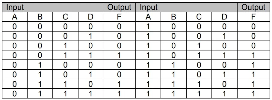
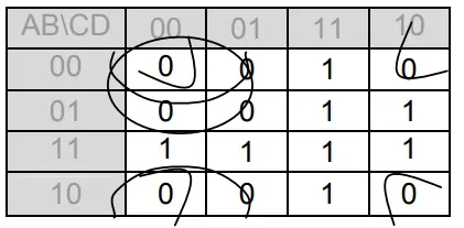
The Adjacent 1s Detector accepts 4-bit inputs. If two adjacent 1s are detected in the input, the output is set to high. The operation of the Adjacent 1s Detector is represented by the function table. In the function table, for the input combinations 0011, 0110, 0111, 1011, 1100, 1101, 1110 and 1111 the output function is a 1.
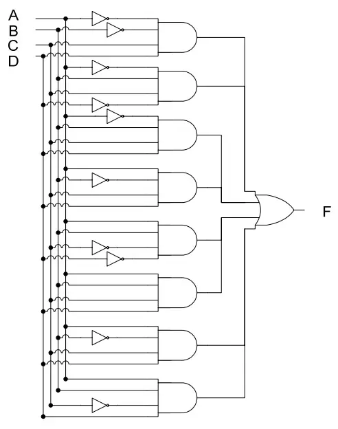
Implementing the circuit directly from the function table based on the SOP form requires 8 AND gates for the 8 product terms (minterms) with an 8-input OR gate.
The total gate count is:
- One 8 input OR gate
- Eight 4 input AND gates
- Ten NOT gates
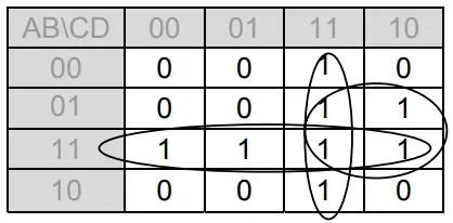
The expression can be simplified using a Karnaugh map, and then the simplified expression can be implemented to reduce the gate count. The simplified expression is ++ BCCDAB . The circuit implemented using the expression ++ BCCDAB has reduced to 3 input OR gate and 2 input AND gates.
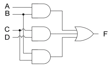
The simplified Adjacent 1s Detector circuit uses only four gates reducing the cost, the size of the circuit and the power requirement. The propagation delay of the circuit is of the order of two gates.
The simplified Adjacent 1s Detector circuit can be implemented using only NAND Gates. The AND-OR combinational circuit can be easily replaced by a NAND based implementation without changing the number of gates.
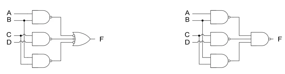
Bubbles representing NOT gates are placed at the output of the three AND gates. Converting the three AND gates to NAND gates. To balance out the three NOT gates added at the outputs of the three AND gates, three bubbles representing three NOT gates are also placed at the three inputs of the OR gate. The Resulting OR gate symbol with three bubbles at the three inputs is an alternate symbol for a three input NAND gate.
Implementing Combinational Logic Circuits using only NAND gates helps in reducing the circuit size and cost as the Integrated Circuit packages multiple gates in a single package. If, for example, the 3-input NAND gate in the circuit had been a 2-input NAND gate, only a single IC package (74LS00) would have been required.
2) POS based Implementation of the Adjacent 1s Detector Circuit
A combinational Adjacent 1s Detector circuit can be implemented, based on the POS form. It was discussed earlier that it is very easy to switch between SOP and the POS representations using the information in a function table or the information mapped to a Karnaugh Map. Referring to the Function Table for the Adjacent 1s Detector. A POS based Adjacent 1s Detector circuit can be easily implemented by using the Sum terms (Maxterms). The POS based circuit for this particular case has 8 sum terms which require 8 OR gates and a single 8-input AND gate.
The total gate count is:
- One 8 input AND gate
- Eight 4 input OR gates
- Ten NOT gates
Both, the SOP based circuit discussed earlier and the POS based circuit give identical outputs for identical set of input combinations. One practical purpose of using either the SOP or the POS based implementation is to reduce the size of the circuit and have a simpler circuit. In the example of Adjacent 1s Detector circuit both the SOP and POS based implementations have equal number of minterms (8) and maxterms (8) thus both implementation use exactly the same number of gates (19). In many cases, the function describing the operation of a combinational circuit has minterms which are either less than or more than the number of maxterms. Thus it is wiser to choose the implementation form that uses the least number of minterms or maxterms to achieve a combinational circuit that uses the least number of gates.
The POS expression can be simplified using a Karnaugh map. The simplified expression can be implemented to reduce the gate count.
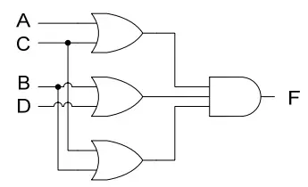
The simplified Adjacent 1s Detector circuit uses only four gates reducing the cost, the size of the circuit and the power requirement. The propagation delay of the circuit is of the order of two gates.
Related Posts:
The simplified Adjacent 1s Detector circuit can be implemented using only NOR Gates. The OR-AND combinational circuit can be easily replaced by a NOR based implementation without changing the number of gates.
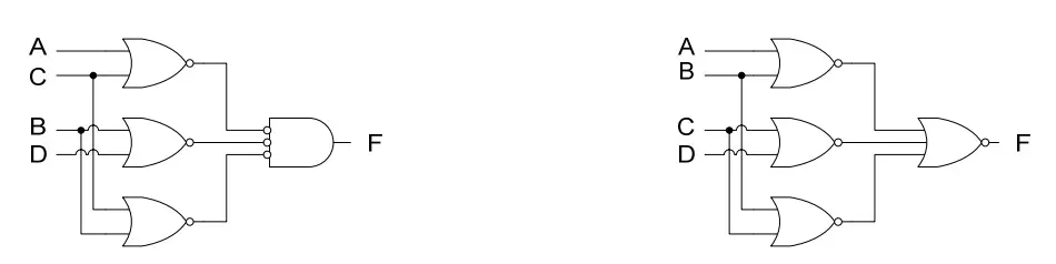
Bubbles representing NOT gates are placed at the output of the three OR gates, converting the three OR gates to NOR gates. To balance out the three NOT gates added at the outputs of the three OR gates, three bubbles representing three NOT gates are also placed at the three inputs of the AND gate. The Resulting AND gate symbol with three bubbles at the three inputs is an alternate symbol for a three input NOR gate.
Operation of Adjacent 1s detector Circuit
The operation of a Combinational Logic Circuit can be verified by applying varying set of signals at the input of the circuit and comparing the output of the combinational circuit with the corresponding outputs in the Function Table. If the varying set of inputs and the corresponding outputs are plotted over a period of time, the timing diagram thus obtained, describes the operation of the circuit.
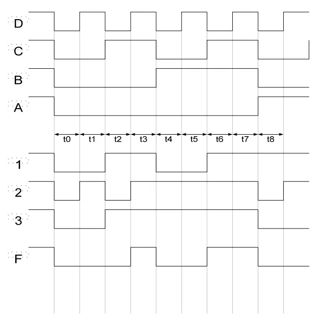
To prove that the SOP and POS based Adjacent 1s Detector combinational circuits synthesized from the Function table.
The timing diagram is for time intervals t0 to t8. A, B, C and D are the inputs to the circuit which are shown changing with time. The timing signals 1, 2 and 3 represent the outputs of the OR gates 1, 2 and 3. The timing signal F represents the output of the circuit.
At interval t0 the input ABCD to the circuit is 0000, the outputs of the three OR gates is 0, 0 and 0 and the circuit output is also 0. At the interval t3 the input ABCD to the circuit is 0011, the outputs of OR gates 1, 2 and 3 are 111. The output F is also a 1, which indicates adjacent 1s. At interval t6 the input ABCD to the circuit is 0110, the outputs of OR gates 1, 2 and 3 are 111. The output F is again 1 indicating adjacent 1s.
The operation of the circuit which is based on the POS simplified expression also proves that a POS based expression determined from the truth table and K-map results in a circuit which operates in an identical manner to that of a SOP based circuit.